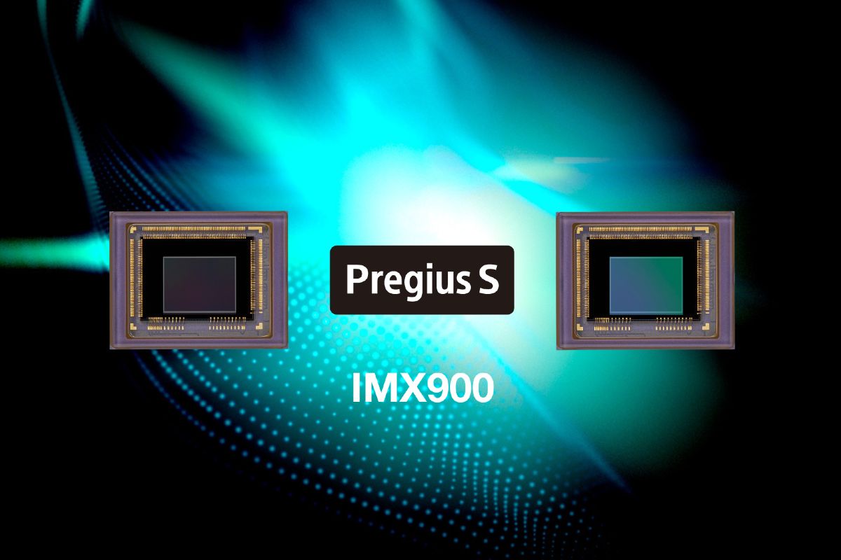
FRAMOS announces the latest launch from Sony Semiconductor Solutions a new global shutter sensor based on its Pregius S™ IMX900.
The Pregius S™ technology leverages Sony’s decades of experience building high quality CCD based sensors to produce fantastic CMOS based sensors with very low noise. These global shutter imagers work very well in high speed, high precision applications like factory automation of assembly lines, traffic, and sports analytics, just to name a few. From there, they flip the chip upside down to place the pixel array closer to the incoming light, creating a distinct back-illuminated structure that enables for smaller pixel sizes and faster frame rates. To make it even more compact, they stack the photodiodes on top of the pixel and signal processing circuits. This enables larger pixel arrays that can fit into smaller optical formats. All these factors have created a suite of global shutter sensors that produce high quality, low noise, large resolution images at very high frame rates at lower costs to camera manufacturers and users.
Pixel Architecture and Enhanced Light Handling in the IMX900 Sensor
The new IMX900 takes this technology one step further by utilizing a new, revolutionary 2.25µm pixel architecture where the individual memory units for each pixel are relocated to the signal processing circuit area, below the photodiode. Most traditional global shutter sensors have these memory units placed beside the pixels which limits the number and size of pixel array. By moving these units below the photodiodes, more and/or larger pixels can now fit into the same area while still maintaining the same saturation capacity. The sensor further improves the incident light angle dependency, allowing for the use of higher aperture lenses without any shading effects.
This imager leverages its deeper pixel wells to provide higher saturation levels with about 10ke- full well capacity and better near IR light performance thanks to thicker photodiode. When this is combined with the changes to the pixel architecture, dramatic improvements can be seen in the quantum efficiency and parasitic light sensitivity in cameras build with this device.
Improved incident light angle dependency simplifies the lens selection or allows for wider lens apertures to significantly increase the light hitting the sensor. For example, reducing the lens by one f-stop down, the amount light entering the camera is doubled so the shutter speed can be half, doubling the output frame rate (FPS). Alternatively, a much better low light performance can be achieved without changing to a shorter shutter time.
IMX900 Sensor: Enhanced for Factory Automation, AGVs, and High-Speed Imaging
The IMX900 was designed with factory automation, AGV/AMR and barcode reading in mind. This 3.2MP, 1/3.1 type imager is available in both color and monochrome formats, and mates nicely with any 1/3” or S-Mount (M12) lens. The sensor supports frame rates of up to 120 fps, higher resolution and double the frame rate of the previous generation IMX296. This keeps camera designs compact which is ideal for handheld applications. On top of this, additional functions can be utilized to further reduce post-processing.
- On Chip Fast AE (Auto Exposure) Function puts the sensor into a very fast frame rate mode to speed up the calculation of image intensity so that precise exposure values can be set to determine the desired image intensity. In this mode, the sensor subsamples the resolution by 1/10 its height to capture images 10x faster with the light intensity analysis being done on the sensor and then, once a final exposure value is achieved, returns to full frame mode to capture the final images. This function speeds up the time needed to determine the overall intensity of the image and complete the exposure adjustments to provide well illuminated final images. Because the AE is done on the sensor, the host platform is not involved in complex calculation allowing for all available computational resources to be dedicated to image processing. On Chip AE can be enabled on demand or can be free run. For example, a camera on an Autonomous Guided Vehicle can very quickly adapt its exposure to compensate for changing ambient light.
- Quad Shutter Mode Function allows individual manipulation of the start of exposure and integration time for each quad pixel of a 2×2 unit, within the capture time of each frame. This allows for either 4 distinct images that each have a different exposure value, or to balance the color response (e.g. white balance) of the camera using exposure times instead of or, as well as, using the sensor color gains. An interesting use case for quad shutter is ultra high-speed shooting applications that allow the acquisition of 4 frames, capturing up to 100,000 fps
- Quad HDR Mode Function leverages the Quad Shutter Mode to set individual exposure times for the pixels within the 2×2 units to provide up to 4 different intensities for the captured images. From there, applications can review these values and interpolate new values to produce high dynamic ranges (HDR) images for challenging lighting conditions. Short and long exposures can be set for these pixels to enable the extraction of information in both the dark and bright regions in one capture without any temporal delay errors being introduced; a common problem found in other multi-image based HDR algorithms. Not only does this improve image performance but it also speeds up image capture as only 1 image is needed to calculate the resultant HDR image.
IMX900 Pixel Architecture
With all these new advancements, it is easy to see that the IMX900 pixel architecture will revolutionize how imagers are built going forward and will open up new applications and dramatically improve existing implementations. You can expect that a new suite of sensors will be based in this technology and will further expand the range of available resolutions allowing for much larger image sizes using smaller, conventional lenses and microlenses. This, in turn, will miniaturize camera designs while reducing BOM costs further allowing them to better target small, low weight IoT and drone applications, and embedded systems looking for large resolution, high speed, images.
