Over the last couple decades, advancements in mobile phone and smart phone camera technology have been at the forefront of developments in complementary metal-oxide-semiconductor (CMOS) technology. In turn, this has driven improvements to both the sensors and the methods for their fabrication. Also during this time, general manufacturing advancements have reduced noise in CMOS sensors and increased their reliability.

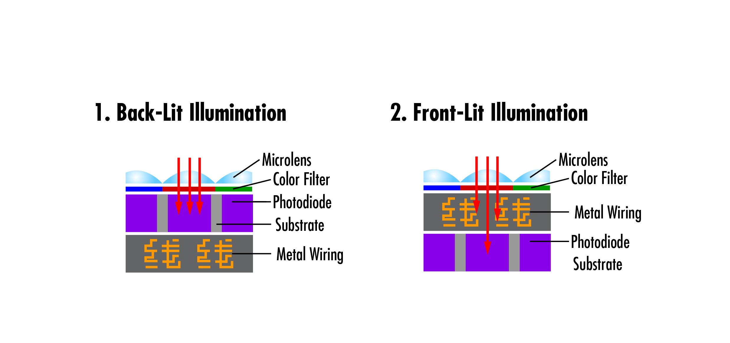
Figure 1: The configuration for a back-lit illuminated pixel and a front-lit
illuminated pixel
One specific alteration consisted of changing CMOS sensor structure from front-lit illumination to back-lit illumination.

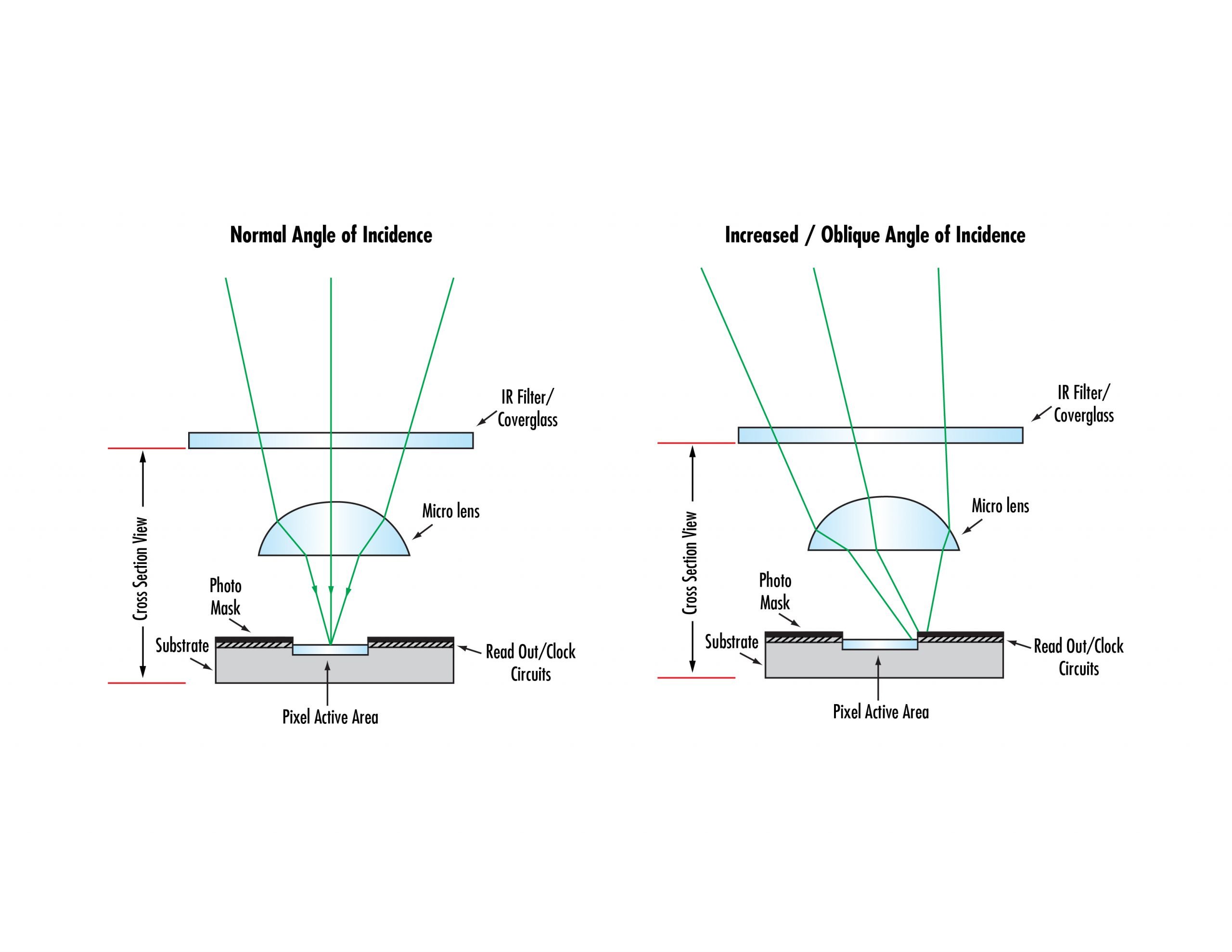
Figure 2: Micro-lenses are used to capture as much light from wider
angles onto the sensor.
Another major improvement to the CMOS sensor design was the incorporation of micro-lenses to maximize the light capture to improve sensor efficiency.
CMOS usage overtakes CCD usage
After these years of technological advancements, the use of CMOS sensors has surpassed the use of charge coupled devices (CCD) for several key reasons. CMOS devices are able to capture images while consuming less power than CCDs, and are less expensive to manufacture making them less expensive (by about a factor of 10) to purchase. By February 25, 2015, CMOS sensor technology was so popular that Sony announced it would cease production of CCD sensor technology
Applications demand higher resolution
As applications become more demanding, higher image quality and resolution are needed. CMOS manufacturers attempted to create sensors with higher resolutions by decreasing pixel size and increasing pixel counts. This was moderately successful; however, it came with some issues, including increased sensor noise. To combat this issue, manufacturers returned to slightly larger pixel sizes but on sensor formats larger than 1.1” sensor formats. This method increased sensor resolution and maintained good signal-to-noise ratios (SNR).


