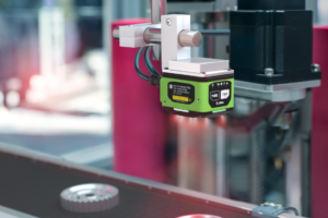
A team of researchers at Nanjing University of Science and Technology, China, has developed an experimental monitoring system capable of detecting dangerous defects in thin-walled 3D-printed parts. At the heart of the setup is a high-speed camera from Mikrotron, which allows scientists to identify “keyhole pores”, microscopic voids that can compromise the strength of parts produced by Laser Powder Bed Fusion (LPBF).
Keyhole pores form when excessive laser energy vaporizes metal, trapping gases that leave behind internal cavities. These pores act as stress points that can crack under pressure, creating the risk of premature failure. With LPBF increasingly used to manufacture lightweight, intricate parts for satellites, aircraft, automobiles, and other demanding applications, catching defects before parts are put into service is critical.
Why Thin-Walled Structures Are Vulnerable
LPBF involves rapid cycles of melting and solidification, creating steep temperature gradients. Thin-walled parts are especially prone to problems, since their small cross-sections concentrate laser energy. While adjusting process parameters can reduce risks, the unpredictable nature of the LPBF layer-by-layer process still leaves room for defects such as pores and deformations.
Traditionally, researchers have used X-ray imaging or other methods to study pore formation. Until now, there has been no practical solution for pinpointing keyhole pores in complex thin-walled structures during production.
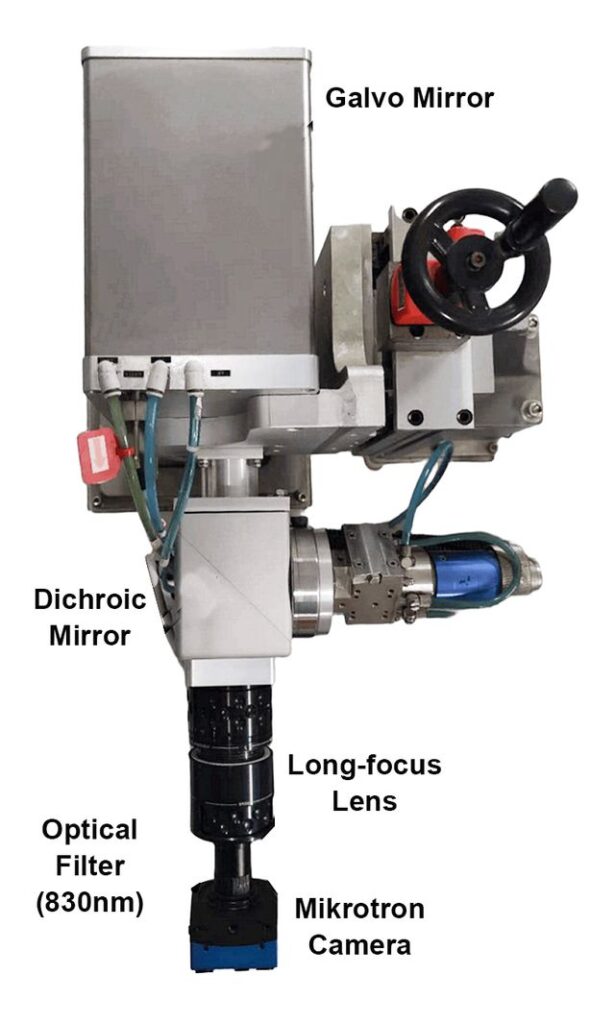
Capturing 10,000 Frames Per Second
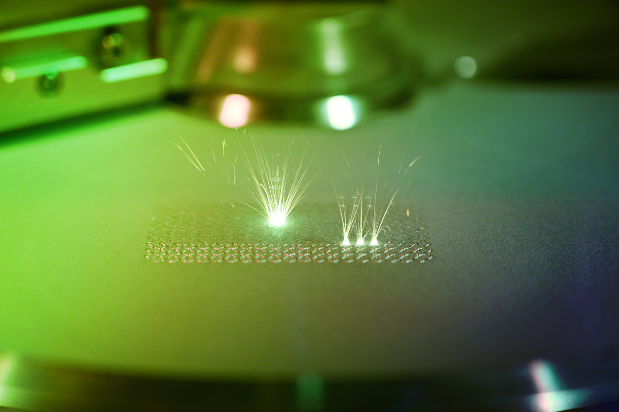
The Nanjing University team’s solution is an in-situ monitoring system that images the melt pool, the area where powder is fused by the laser, in real time. The system relies on the Mikrotron EoSens MC1362, a CameraLink™ CMOS color camera. While capable of 500 frames per second at full resolution, the camera was configured for 160 x 160 pixel images at a remarkable 10,000 fps, with a resolution of 9.85 μm per pixel.
The imaging setup includes a dichroic mirror and bandpass filter to isolate melt pool emissions, while a galvanometer scanner records laser beam coordinates at the same speed. Synchronizing these two data streams allows researchers to map melt pool activity directly to precise build locations.
Because processing 10,000 images per second is computationally intensive, the team added an NVIDIA RTX 4090 GPU with CUDA acceleration. They also applied Principal Component Analysis to streamline feature extraction, reducing memory and processing demands.
Accuracy Above 95%
The results were striking. The model achieved 95.82% accuracy in predicting pore locations, even across parts with varying wall thicknesses and overhang angles. The study also found a strong link between melt pool intensity and surface roughness, both of which drive pore formation.
According to the researchers, this breakthrough lays the foundation for real-time defect monitoring in LPBF, opening the door to safer, more reliable production of critical aerospace and automotive components.
Learn more at www.mikrotron.de or www.svs-vistek.com.