Maximilian Klammer, Research & Develop Manager and Klaus Riemer, Project Manager at Chromasens, explain how to meet the demands of semiconductor inspection with CMOS Color Line Scan Cameras.
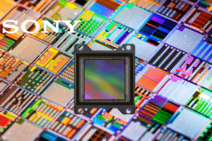
Semiconductor geometries and printed circuit board (PCB) components are becoming smaller, while the demands on quality testing and control are growing. Because of the minute structures involved, optical inspection in modern semiconductor manufacturing occurs in the micrometre range. The need to detect defects and contamination at this scale and at high throughput places the highest demands on inspection systems. Extremely high-resolution colour line scan cameras with CMOS technology have been developed to accomplish this.
CMOS Technology
Line scan cameras are suitable for image-capturing tasks where fast-moving large areas or flat objects must be captured and analysed with high optical resolution. In a CCD line scan camera, the pixels of the sensor are arranged in a single line. The readout cycle is adapted to the throughput speed of the inspected objects or surface areas. The whole two-dimensional image is then created by joining the individual lines together.
CCD sensors have long been the technology of choice in line scan imaging because of their image quality, high sensitivity, low noise, low photo-response non-uniformity (PRNU), high dynamic range, and signal-to-noise ratio. These benefits are essential in line scanning because of the high-speed image acquisition and reduced number of photosensitive cells, which means exposure is limited.
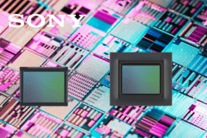
New-generation CMOS line scan sensors now offer similar image quality to CCDs, coupled with benefits such as higher readout speed and flexible readout modes. Unlike single-line CCDs, these sensors have several lines of pixels, allowing for different operation modes depending on an application’s requirements. One key benefit of a multiline sensor is time delay integration (TDI). TDI consists of adding up the values of adjacent pixel lines synchronously with the motion of the object below the camera. The same section of the object is imaged by several lines, and adding up the signals of all these lines increases the signal intensity compared with a single-line sensor. This solution has a much better signal-to-noise ratio than an equal increase in gain.
The trend toward miniaturisation continues for PCBs and the components mounted on them. This leads to so-called penalisation, whereby several PCBs are manufactured on one panel. Each PCB on the panel is identified by a unique barcode, and thus rapidly inspecting the PCBs is correspondingly complex and demanding. For example, during the visual inspection, existing solder defects, such as interruptions, solder bridges, solder short circuits, or excess solder, must be identified, in addition to component defects such as lifted solder and missing or misplaced components. A colour line scan camera system can perform these inspection tasks with great accuracy because of its high operating speed and lateral resolution.
Oxidised copper wires on PCBs must also be detected, yet monochrome systems cannot reliably identify oxidised areas. However, high-performance colour line scan cameras such as the allPIXA evo from Chromasens, combined with high-performance illumination, excel at this task.
Examples from semiconductor and PCB manufacturing show that high-performance colour line scan cameras can play an important role as central components in 100% real-time inspection processes. The image quality and resolution performance of multiline full-colour CMOS line sensors results in a particularly high application potential for camera systems. Fast and accurate colour measurements and rapid 3D inspection are additional future applications.