In a major stride for optical sensing and imaging-system reliability, SI Sensors, the CMOS image-sensor design arm of Specialised Imaging, has formally unveiled its next-generation hermetic packaging solution—engineered to significantly extend device lifetimes and performance in the most extreme environments. The advanced vacuum-sealed enclosures are being hailed as a substantial improvement in protecting CMOS sensors from environmental contaminants, mechanical stress, and thermal loads, and could find applications in sectors ranging from space exploration to ultra-high-speed industrial imaging.
Hermetic Packaging: The Next Frontier
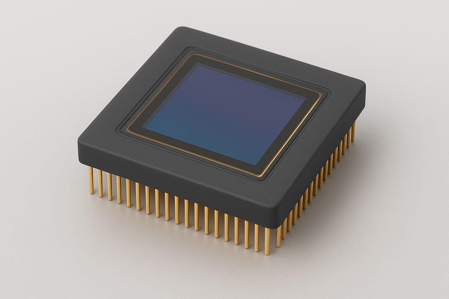
At the heart of the innovation are ceramic-to-metal and sapphire-to-metal seals proven, yet refined with greater precision and integration with advanced optics components. Ceramic materials bond to metal housings with excellent vacuum integrity and mechanical durability, while sapphire windows deliver both extraordinary hardness and exceptional optical clarity, covering the ultraviolet (UV) through infrared (IR) spectrum with minimal absorption or distortion. Notably, SI Sensors has achieved sub-micron precision die placement, a level of alignment that streamlines integration with high-performance optics and maximises the active area, all while minimising aberration or misalignment. Enhanced thermal conductivity built into the packaging further ensures reliable heat dissipation critical for ultra-high-speed or high-power sensors whose performance can degrade rapidly with rising junction temperatures.
“Hermetic packaging is more than just a containment strategy it is a performance enabler”
Philip Brown, General Manager of SI Sensors
“Our new designs safeguard custom CMOS image sensors in conditions where failure is simply not tolerated, from the vacuum of space to contaminant-laden industrial processes. These packages enable consistent operation over extraordinarily long periods, even under the harshest demands.”
Applications and Implications
The implications of such technology are wide-ranging: Space and aerospace: CMOS sensors encapsulated in vacuum-sealed, radiation-resistant packages are ideal for satellite payloads, planetary rovers, and astrophysical observatories. In space, with its wide temperature swings, radiation exposure, and vacuum conditions, both sealing integrity and thermal management are paramount. Scientific instrumentation: High-energy physics detectors, synchrotron beamline imagers, and nuclear imaging systems benefit when sensors maintain calibration and sensitivity over time, despite exposure to particulate contamination, vacuum or semi-vacuum environments, and extreme UV or X-ray radiation. Ultrafast industrial imaging: Process monitoring in semiconductor fabrication, combustion diagnostics, or ballistics testing often places sensors in environments with corrosive gases, particulates, or rapid thermal cycling. A hermetic, thermally conductive enclosure extends lifetime and reduces calibration drift, thereby improving throughput and reducing downtime.
Hermetic Packaging in Context
Hermetic packaging is not new per se, it’s long been employed in fields such as aerospace, military electronics, and medical implants. However, recent developments have pushed boundaries on multiple fronts: Materials and Sealing Techniques: Ceramic-to-metal and glass-to-metal seals have proliferated, but sapphire-to-metal seals are gaining traction due to their broad optical transparency and mechanical resilience. Miniaturisation of MEMS and Image Sensors: As device sizes shrink and pixel pitches decrease, even sub-micron misalignment in packaging can degrade performance, making precision die mounting more critical than ever. Integrated Photonics and Hybrid Systems: With growing interest in integrated optical systems (combining lenses, filters, micro-optical elements), packaging must accommodate more complex optical stacks—sapphire provides excellent substrate compatibility for these. Reliability and Lifetime Requirements: In demanding industries, failure rates must remain below parts per million, even after thousands of hours in harsh conditions. Truly hermetic packaging is essential to meet such reliability standards.
Inside SI Sensors
SI Sensors brings together an entire suite of capabilities, from circuit design to full cryogenic, thermal, mechanical and electro-optical testing. Its offering spans: Custom CMOS sensor circuit and pixel design; Simulation, layout, verification, and tape-outs across global foundries; Electro-optical characterisation (noise, dynamic range, quantum efficiency); Mass-production testing and quality assurance, aligned with standards such as EMVA 1288 (a comprehensive framework for measuring and comparing the performance of image-sensor systems). The new hermetic packaging now complements these capabilities, ensuring that the sensors not only perform at the lab-bench level but also endure the rigours of deployment in unforgiving environments.
Academic and Industrial Response
Experts in sensor reliability highlight that the challenges SI Sensors is tackling are pressing and widespread. According to a recent review in IEEE Transactions on Device and Materials Reliability, contamination ingress and thermal fatigue are among the leading causes of image-sensor failure in industrial and aerospace applications. Improved hermetic sealing paired with effective thermal paths can significantly extend mean-time-to-failure (MTTF). Similarly, a 2024 paper in Sensors journal underscored that sapphire windows in imaging systems provide over 90% transmission from 190 nm (deep UV) to 5 µm (mid-IR)—a benefit for multi-spectral sensing. By combining vacuum-integrity sealing, optical transparency, mechanical robustness, and thermal management in one platform, SI Sensors’ new packaging addresses all these reliability vectors in a unified solution.
What Comes Next?
SI Sensors indicates that the new hermetic packages are available now for inclusion in upcoming sensor projects—either in prototypes for research institutions or rapidly scaling into production volumes. The firm highlights that the packaging is designed to be versatile, compatible with multiple CMOS architectures (global-shutter, rolling-shutter, high-dynamic-range, etc.) and sensor formats. Looking forward, deployment in real-world trials—such as high-altitude balloon payloads, in-line industrial camera systems, or even lunar lander payloads—should validate long-term performance. Combined with the sensor’s in-house verified performance (noise, gain, quantum efficiency, linearity), the hermetic enclosure could unlock new use cases where previously custom sensor designs were thwarted by environmental limitations.
SI Sensors’ introduction of next-generation hermetic packaging represents a substantial advancement in CMOS image-sensor reliability. By integrating sapphire and ceramic-to-metal sealing, sub-micron die alignment, and superior thermal pathways, the firm addresses critical failure modes in some of the most demanding operational domains. As imaging technologies continue penetrating fields like space science, industrial automation, and scientific instrumentation, such ruggedised, high-performance solutions will likely become as vital as the sensors themselves. In a world increasingly reliant on vision and data, packaging innovations like these could be the unsung enablers of tomorrow’s breakthroughs.
For further information please visit www.si-sensors.com or contact the company on +44 1442 827 728 / info@si-sensors.com,