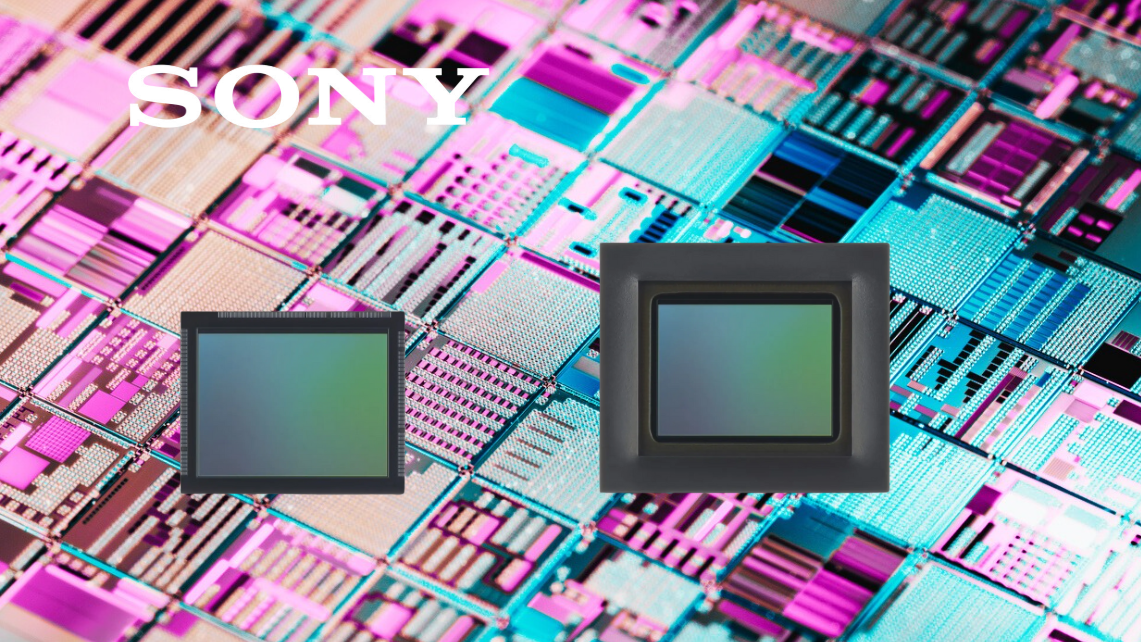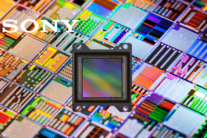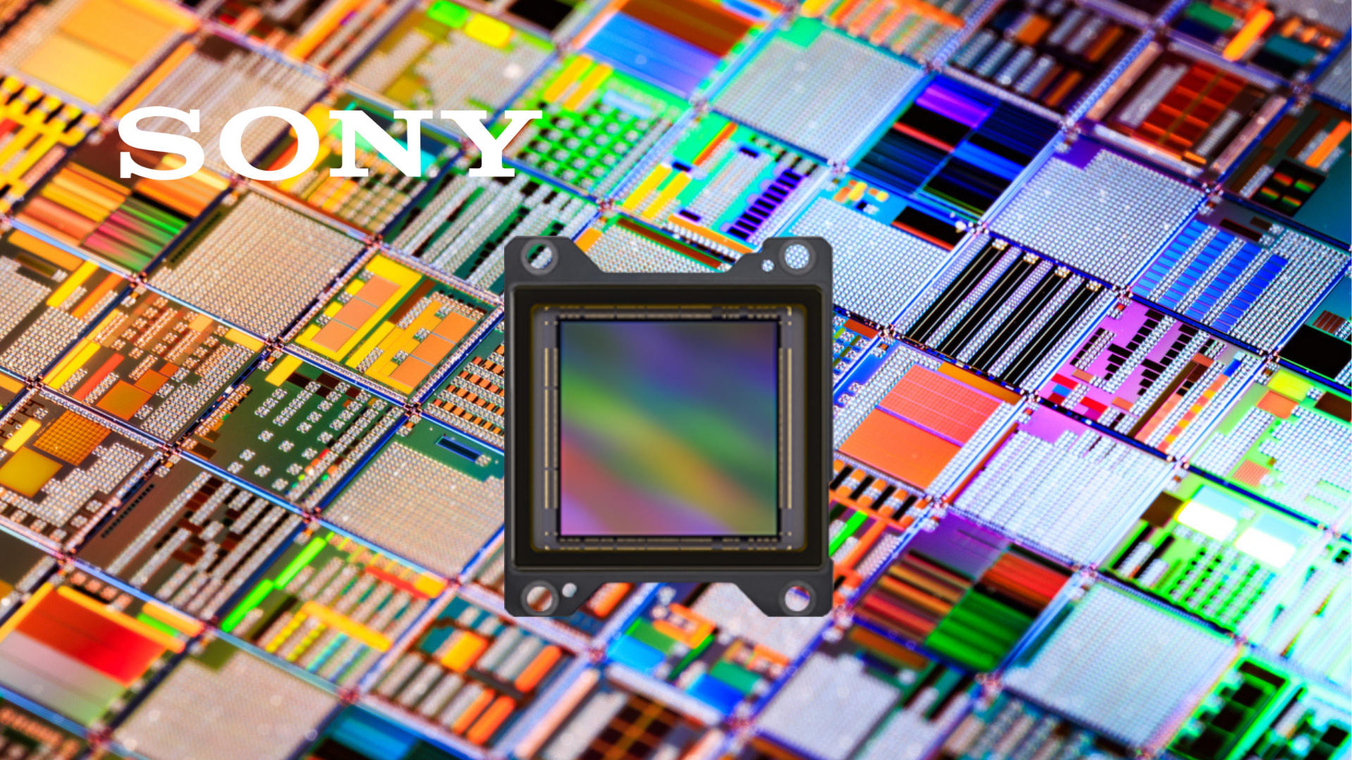
Sony’s IMX927: A New Standard for High-Speed, High-Resolution Industrial Imaging
September 29, 2025 marked a significant milestone in the world of imaging technology as Sony Semiconductor Solutions announced the IMX927, a global shutter CMOS sensor boasting 105 effective megapixels and the ability to capture at up to 100 frames per second.
For industrial and machine vision applications, where both speed and clarity are critical, this sensor has the potential to shift what engineers and integrators can expect from image capture systems.
Breaking the Resolution-Speed Trade-Off
Traditionally, system designers have faced a difficult choice: opt for ultra-high resolution at the cost of speed, or prioritize frame rate and sacrifice detail. The IMX927 challenges that compromise by combining over 100 megapixels of detail with global shutter technology at industrial frame rates.
For machine vision professionals, this means large areas can be inspected in real time with fewer passes or fewer cameras. Tasks such as flat panel inspection, wafer metrology, or high-precision robotics benefit from the ability to capture more detail, more quickly, without distortion.
Built for Industrial Realities
At the core of the IMX927 is Sony’s Pregius S™ global shutter pixel technology, which eliminates rolling shutter artifacts and ensures distortion-free images even in high-vibration or high-speed scenarios. In environments such as automated assembly lines or robotics-driven inspection systems, this reliability is essential.
Equally important is the sensor’s stacked, back-illuminated design, which maximizes light collection and keeps noise levels low, even as pixel sizes shrink. This ensures the IMX927 performs in the challenging lighting conditions often found in industrial settings.
More Than Just a Sensor
Sony has also designed the IMX927 with system flexibility in mind. A new ceramic package with connectors allows for easier integration and potential sensor swapping, giving camera manufacturers and system integrators a more modular platform to build on. This is a forward-looking design choice that reflects the needs of a market demanding longer system lifecycles and upgradable architectures.
Applications Across Industries
The sensor’s specifications open the door to a range of industrial and scientific applications:
- Semiconductor and flat panel inspection: Detecting the smallest defects on wafers and displays at speed.
- 3D metrology and measurement: Enabling faster structured light or scanning systems for precise surface mapping.
- Robotics and automation: Providing high-quality, distortion-free imaging in dynamic production environments.
- Motion analysis: Supporting detailed vibration studies and performance diagnostics in aerospace and automotive testing.
Looking Ahead
Sony expects sample shipments of the IMX927 to begin in mid-November 2025, with camera makers likely to showcase first implementations in early 2026.
The launch underscores Sony’s continued dominance in the industrial imaging sector, but it also raises expectations for the wider ecosystem. Competing sensor makers will be under pressure to match the IMX927’s blend of speed and resolution, while camera and system integrators will be eager to see how this technology can be leveraged to improve performance and efficiency in machine vision systems.
In short, with the IMX927, Sony has not just launched another sensor. It has set a new benchmark for what’s possible in industrial vision, combining scale, speed, and reliability in a way that could redefine high-end imaging for years to come.
Read more at https://www.sony-semicon.com/en/products/is/industry/gs/imx927-937.html